
Dropping thousands on new PC gear often gets me thinking philosophically (especially with all of the quiet time during benchmark runs!) It is easy to get caught up in the specification holy wars of AMD Excavator vs Ivy Bridge, Tahiti vs Kepler, etc. and lose sight of just how far desktop computing power has come. Reviewing the architecture of the GTX Titan really brought this point home.
Consider for a moment, the NVidia SMX, or Streaming Multiprocessor Next Generation. This is the brains of the operation for the current Kepler generation of NVidia GPUs. Here is a snapshot of the internal architecture of the GK110 SMX (GTX Titan variety):
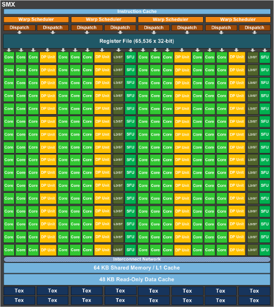
What an incredible piece of technology! You essentially have an entire high performance computing grid on a single die with the SMX. There are 192 CUDA cores (Compute Unified Device Architecture). These are fully programmable, massively parallel, computing cores design to operate slowly and steadily on a huge number of threads (by contrast, fully general purpose architectures like Intel x86 feature core designs that are designed to work on a much smaller number of threads, but much more quickly). The reason behind this architectural difference is very much tied to their intended purpose. A general purpose CPU like an Intel x86 part is designed to run general operations. Lots and lots of small blocks of instructions, with a ton of repetition, all of which are time sensitive and loosely interdependent, operating on small, disparate, sets of data. For example, on a typical day you might have your email client up in a web browser, which continually opens network sockets and receives small amounts of data from the network interface triggering a minor UI update in a browser. At the same time you might be working on creating a document in a productivity application which continually scans the keyboard and mouse for input, captures data from the user, responds to user requests interactively, and saves data to the storage system interface steadily. In the background, the multi-tasking operating system is running and continually doing housekeeping which interacts with, and manages all of these interfaces (network, disk, IO) to keep the environment healthy.
Now consider the job of the GPU. There is a massive amount of data (the flow of images to be rendered) and a well defined process with very sticky interdependency which operates on it (the 3D pipeline). Any loss can stall the pipeline entirely which causes a high level of disruption in the user experience. Smooth but slower, in other words, is better than faster but jerky. A system like this requires lots of computing units that can take this predictable, and well defined, pattern and work on it in parallel as quickly (and consistently) as possible.
So 192 of these guys work together in a GK110 (GTX Titan). What they do is floating point math, most of the time. Tons of floating point math because that’s what 3D spatial calculations require (makes sense). Most of these calculations, for a game, are “single precision” floating point since the bulk of the calculations are reasonably simple. This is good because an SP computing part can be smaller and less complex than a “double precision” one since double precision floating point calculations require more computational power and, hence, more transistors and circuit paths. Using single precision computational units to do double precision calculations is super inefficient, however. And sometimes, double precision calculations do come up. That drag on efficiency slows every thing down since the system is highly interdependent. To rectify this, the GK110 also includes 64 dedicated double precision computing units on the same die. Thats a crazy number of 256 floating point computing units on one die. But that’s not all!
Looking at the diagram, you can see that in addition to the single, and double, precision floating point units, there are also SFU’s or “special function units” and “texture units”. The texture units are directly responsible for the texture mapping phase of the 3D pipeline (where bitmapped image data is applied to a rendered 3D surface). The “special function units” are directly responsible for “transcendental functions” or, basically, trigonometric math (sin, cos, tan, etc). There are 32 of these SFUs. Tying all of these components together are 32 load/store units used to move data in and out of memory, a common network bus for component intercommunication, a shared block of discrete data and instruction cache, a bank of dispatch units that issue instructions to the computational units, and a scheduler that runs the show. Overall just an incredible piece of technological achievement. It could be argued that the single SMX is more complex than an entire, multi-core, general purpose CPU like an Intel Sandy Bridge processor. And get this… A GTX Titan has 14 of these SMX units on it’s board all sharing 6GB of incredibly fast RAM. Let’s take a quick, sobering look, and what all of these specs add up to in real-world capabilities (straight from NVidia):
GTX TITAN GPU Engine Specs:
- CUDA Cores 2688
- Base Clock (MHz) 837
- Boost Clock (MHz) 876
- Texture Fill Rate (billion/sec) 187.5
GTX TITAN Memory Specs:
- Memory Clock 6.0 GbpsStandard Memory Config 6144MB
- Memory Interface GDDR5
- Memory Interface Width 384-bit GDDR5
- Memory Bandwidth (GB/sec) 288.4
For anyone who is even slightly familiar with computing capabilities, those are really jaw dropping numbers. 288GB/sec of memory bandwidth? I mean seriously?! By comparison the also super impressive Sandy Bridge E on Intel x79 chipset gives you 50GB/s of bandwidth using quad-channel 64bit DDR3 running at 1600Mhz. Now of course on a GTX Titan there are, once again, 14 super dense computing units sharing that memory bus all cranking along at 1Ghz under load yielding that staggering 187 billion texture per second fill rate.
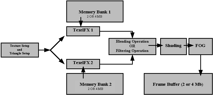
- Voodoo2 (V2 1000) 90 MHz clock (memory and core)
- 135 MHz RAMDAC,dithered 16-bit (65536 color) display.
- Full-screen, 3D-Only accelerator, works with another 2D or 2D/3D VGA card through a VGA pass-through cable. Picture softened slightly by analogue VGA pass-through cable.
- Resolution up to 800 x 600 and higher resolution through SLI, (Scan Line Interleave) up to 1024 x 768.
- Supports 8 or 12 Megabytes high speed EDO DRAM rated at 100MHz but running at 90 MHz, 25 ns.
- RAM configured into 4 Megabytes for frame buffer(s) and Z-buffer and 4 or 8 Megabytes texture memory.
- 90 million fully featured pixels/sec sustained fill rate for bilinear textures, with LOD MIP-mapping, Z-buffering, alpha-blending and fogging enabled).
- 3 Million fully featured triangles/sec (Filtered, LOD MIP-mapped, Z-buffered, alpha-blended, fogging enabled, textured triangles).
- 180 Million pixel/sec with scanline interleaved configuration.
- Bi-linear and tri-linear texture filtering.
- Level of Detail (LOD) mipmapping
- Supports Multiple textures per pixel.
- Bump mapping through texture composition.
- Edge Anti-aliasing.
- Hardware triangle set-up (independent strips and fans).
- Perspective, Sub-pixel and sub-texel correction.
- Ground shading and texture modulation.
- Z-buffering (16bpp, integer and floating point).
- alpha blending and fogging
- Linear frame buffer access.
- Single-pass tri-linear filtering.
- Single-pass dual textures per pixel.
Again… Wow. Lets do a quick comparison:
| 3DFX Voodoo 2 | GTX Titan | |
| Compute | ||
| Processors | 3 | 14 |
| Cores | 3 | 4704 |
| Clock Rate | 90Mhz | 1Ghz |
| TFLOPs | come on now! | 4.5 |
| Fill Rate | 90M pixels/s | 187B pixels/s |
| SLI | 2 | 4 |
| VRAM | ||
| Type | EDO DRAM | GDDR 5 DRAM |
| Size | 12MB | 6GB |
| Speed | 2.1GB/s | 288GB/s |
| Original MSRP | $279 | $999 |
In 15 years state of the art 3D has made a truly revolutionary leap. The GTX Titan has so much more computational power than the original 3DFX Voodoo 2 that it is almost difficult to draw a reasonable comparison. The increase is literally multiple thousands of times in pure computational power and hundreds of times the RAM footprint. When you consider that the price has only increased by about 350% the $999 Titan almost seems reasonable!

Psycho approves of big honkin’ GPUs!
